Bonding Silicon Wafers for Silicon-on-Insulator

-
 July 8, 2024
-
 WaferPro
-
0


WaferPro has over 10 years of experience with advanced wafer bonding processes and technologies for fabricating high-quality silicon-on-insulator (SOI) wafers. As pioneers in this field, we have developed innovative techniques for bonding silicon wafers that enable our customers to manufacture SOI devices with exceptional performance.

How Wafer Bonding Works
Wafer bonding is the process of joining two semiconductor wafers through direct surface contact to produce a single composite wafer for device fabrication. There are two primary wafer bonding methods WaferPro utilizes for SOI manufacturing:
- Direct Silicon Bonding (also called Fusion Bonding)
- Anodic Bonding
Direct Silicon Bonding
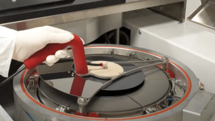
Direct silicon bonding fuses two silicon wafers together without any intermediate glues or bonding agents. The wafers are cleaned, conditioned, and brought into physical contact at room temperature to initiate the bond through hydrogen bridges and van der Waals forces. Then, the stack is annealed at high temperatures (>1000°C) so that silicon atoms on the two surfaces interdiffuse and form a single robust silicon crystal across the original boundary.
Anodic Bonding

In anodic bonding, one of the wafers has a borosilicate glass layer that, when heated and placed under an applied voltage, chemically bonds to the silicon wafer placed on top of it. This glass layer in the final SOI wafer serves as the insulating buried oxide layer that silicon devices are fabricated on top of.
Summary of Bonding Methods
| Bonding Method | Bonding Mechanism | Key Process Details |
|---|---|---|
| Direct Silicon Fusion Bonding | Siloxane linkages form covalent Si-O-Si bonds during annealing | Ultra-smooth, clean, particle-free surfaces. Critical annealing step > 1000°C |
| Anodic Bonding | Electrostatic attraction and O- transport creates chemical bonds between glass and silicon | Heat + high DC voltage. Borosilicate glass layer |
Both direct and anodic bonding produce extremely strong and stable interfaces ideal for SOI applications. At WaferPro, we leverage advanced surface preparation, automation, and statistical process control to achieve bond strengths >1 J/m² with excellent uniformity across every bonded SOI wafer.
Silicon Surface Preparation
Achieving reliable, high-strength wafer bonding requires exceptional surface quality and cleanliness before bringing the wafers into contact. WaferPro has refined wafer surface preparation into a robust science through proprietary enhancements of industry-standard RCA cleaning procedures.
Our advanced RCA cleaning process includes additional steps for:
- Particle and metal ion removal
- Organic contamination elimination
- Oxidation and oxide stripping
- Defect etching
- Final surface passivation
These meticulously designed cleaning sequences reduce wafer surfaces to their elemental silicon state while removing all possible sources of particles and contamination from previous processing. This renders the surfaces hydrophilic and ready for intimate bonding interactions.
We also employ special sacrificial bond and de-bond metrology test wafers to verify surface cleanliness, smoothness, and bondability prior to fusion. Our stringent analytics ensure every production wafer meets specifications before loading into the bonder. This physics-based approach is essential for achieving high first-pass yields.
Key Surface Metrics for SOI Bondability
- Particles >100nm: Zero
- Surface roughness (RMS): <0.15 nm
- Flatness (TTV): <1 μm
- Surface chemistry (contact angle): Hydrophilic (<20°)
Through substantial engineering efforts centered on surface science, WaferPro has developed silicon wafer bonding processes that meet these stringent requirements for bonding high-quality SOI production wafers.
Automated Production Tools
Delivering repeatable, high-yielding SOI wafer bonding requires state-of-the-art automation designed specifically for silicon fusion processes. WaferPro operates an installed fleet of latest-generation automated bonders engineered around key elements of our process innovation:
- Ultra-clean vacuum environment: Prevents any particle or contamination from getting between wafers during bonding. Bonder chambers baseline at 5 nTorr.
- Surface profiling and nanotopography: Built-in optical interferometers scan every wafer prior to bond, generate 3D surface maps, and confirm parameters before initiating bond cycle. Ensures specification compliance.
- Precision wafer handling: End effectors and motion systems designed specifically for thin, bare silicon wafers. Minimizes any handling defects, particle generation, or edge chipping during bonding.
- Real-time bond initiation detection: Allows active measurement of intrinsic bonding phenomena like desorption, contact wave propagation, and healing layer formation. Guarantees cycle recipe parameters optimized.
- Environmental controls and monitors: Precisely regulates chamber temperature, atmosphere, and force variations to within tiny fractions over the entire bond timeline. Critical for process stability.
These engineered elements of WaferPro's automated bonding cluster tools enable unprecedented quality control over every bonded SOI wafer. Combined with our rigorous factory information systems and advanced process control solutions, we ensure steady-state manufacturing of SOI substrates with industry-leading uniformities and yields.

Metrology for SOI Quality Assurance
To deliver exceptional SOI bonded wafer quality to our customers, WaferPro employs a comprehensive analytical methodology consisting of several destructive and non-destructive inspection tools focused on metrics key to SOI device performance:
- Bond Strength Testing
- Crack Opening Method
- Insertion Method
- Surface Morphology
- Laser-based inspection
- AFM Scanning
- Film Thickness Mapping
- Spectral Reflectometry
- Ellipsometry
- Crystalline Defects & Material Quality
- X-Ray Topography
- TEM Imaging
Our pioneering work developing many of these analytical techniques specifically for SOI enables our team to rapidly diagnose and resolve any deviations from standards observed during mass manufacturing. This high sampling rate combined with advanced automation gives WaferPro the capability to supply SOI substrates with <1% bonded interface defectivity routinely.
SOI Customization
Aside from industry-leading quality and bond uniformity, what sets WaferPro apart is our engineering team's ability to customize SOI wafers to meet customers' specific device performance requirements. Over our 20+ years as specialized SOI experts, we have developed and qualified over 1000+ unique SOI wafer configurations. This technology portfolio built on real customer learning is unmatched in the industry.
Key SOI Customization Options
WaferPro enables customers to select from a wide range of layer thicknesses, handle wafers, buried oxide options, and other parameters to optimize their SOI substrate for end application requirements. Some of the key customizations we offer include:
- Silicon Device Layer
- Thicknesses: 20 nm to 300 μm
- Doping: n-type, p-type, float zone
- Crystal orientation: 100, 110, 111
- Buried Oxide
- Thicknesses: 50 nm to 3 μm
- Oxide material: SiO₂, SiNx, Al₂O₃
- Handle Wafer
- Diameter: 2" to 300 mm
- Material: Si
- Bond Interfaces
- Patterned/textured surfaces
- Interlayers for backend integration
With our Pilot Line capabilities, we also support customer process development by providing engineering-grade SOI wafers. This enables rapid prototyping and demonstration of next-gen SOI device architectures.
Business Benefits
By leveraging WaferPro's SOI expertise and customization experience, customers can realize major cost and technology benefits:
- Accelerated Time-to-Market
- Prototype SOI designs
- Seamless transfer to volume production
- Lower Development Costs
- Eliminate in-house SOI tooling investments
- Leverage existing SOI technology portfolio
- Focus R&D Resources on Core Differentiation
- Outsource SOI substrate manufacturing
- Redirect valuable headcount to device innovation
Please contact our technical team to discuss your custom SOI requirements and how WaferPro can provide the optimal solution.
The Future of Advanced SOI
As silicon devices continue advancing towards the limits of traditional CMOS gate pitches and architectures, next-generation technologies like FinFETs and Gate-All-Around nanosheet designs rely heavily on SOI's performance-boosting properties.
Additionally, market segments like radio frequency (RF) and power conversion stand to benefit enormously from integrating devices onto application-specific SOI substrates.
WaferPro continues leading the way on commercialization efforts for these advanced technologies through strategic R&D programs focused on:
- Novel multi-stack 3D and lateral SOI integrations
- Heterogeneous multi-material substrate engineering
- Ultra-thin SOI for new transistor topologies below the 5nm node
- Large-area microchip integration techniques
We also partner directly with industry and academia on research into future high-speed, low-power electronic systems that leverage our expertise in advanced substrate technologies like SOI. Please inquire about joint development opportunities that utilize WaferPro's state-of-the-art SOI manufacturing infrastructure and process know-how.
Having already pioneered many of the FOx and SOI product families and configurations popular in leading-edge devices today, WaferPro stands ready to co-develop and manufacture the next generation of engineered substrate solutions powering tomorrow's innovations. Please contact us with any questions or to discuss your project's technical substrate requirements.

Can’t find wafers that meet your desired specs? No problem! We can build wafers with unique specifications to meet your needs.
Request a quote


Our online store features a wide variety of wafer sizes, orientations, dopants, thicknesses, and more.
Shop online
-
 1286 Alma Ct, San Jose, CA 95112
-
 + 1 408 622 9129
-
sales@waferpro.com
-
Monday – Friday,
9:00 a.m. to 6:00 p.m.


